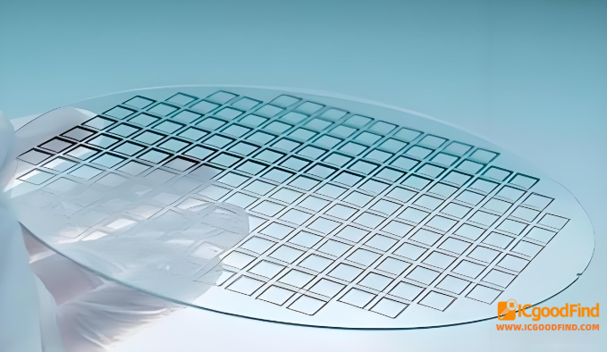
On July 24, Jiaxing Semiconductor announced that its homogeneous thick-film gallium oxide (β-Ga₂O₃) epitaxial wafers have passed full device verification at Xidian University, where SBD Schottky barrier diodes without termination structures were fabricated and tested.
The test used 10μm epi-layer thickness with 1×10¹⁶ cm⁻³ carrier concentration. Results showed breakdown voltage of 1090–1490V, significantly exceeding Japanese peer products – confirming low defect density and excellent wafer quality for ultra-high-voltage power device applications.
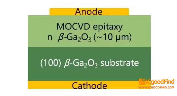
Specific on-resistance measured between 2.6–4.5 mΩ·cm², also outperforming Japanese counterparts, proving the material simultaneously achieves high blocking voltage and low conduction loss – a balanced combination critical for high-efficiency power conversion.
Jiaxing noted that the verified data exceeds imported materials across key metrics, confirming the competitiveness of domestic gallium oxide epitaxial wafers. The product is now available for spot supply, supporting R&D and mass production downstream.
From ICgoodFind: Gallium oxide just outscored the global benchmark – in both breakdown and conduction. This means Chinese wide-bandgap materials are no longer followers; they’re setting the standard for next-gen high-voltage power chips.